Patent application title: Optical transmission assembly
Inventors:
Akihiro Hiruta (Hitachi, JP)
Assignees:
HITACHI CABLE, LTD.
IPC8 Class: AH01S308FI
USPC Class:
372 99
Class name: Particular resonant cavity specified cavity component reflector
Publication date: 2009-07-02
Patent application number: 20090168830
Inventors list |
Agents list |
Assignees list |
List by place |
Classification tree browser |
Top 100 Inventors |
Top 100 Agents |
Top 100 Assignees |
Usenet FAQ Index |
Documents |
Other FAQs |
Patent application title: Optical transmission assembly
Inventors:
Akihiro Hiruta
Agents:
MCGINN INTELLECTUAL PROPERTY LAW GROUP, PLLC
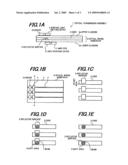
Assignees:
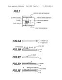
Hitachi Cable, Ltd.
Origin: VIENNA, VA US
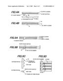
IPC8 Class: AH01S308FI
USPC Class:
372 99
Abstract:
An optical transmission assembly consists of an upper cladding; a lower
cladding; a specified width core formed between the upper cladding and
the lower cladding; a surface light emitting device mounted on an upper
surface of the upper cladding, a light emitting surface of the surface
light emitting device facing the core; a reflective surface formed at a
position in the core facing the light emitting surface of the surface
light emitting device, and inclined in a longitudinal direction of the
core; a shift area formed by which a beam from the light emitting surface
of the surface light emitting device and the reflective surface are
shifted in a width direction of the core relative to each other; and a
light receiving device mounted on a lower surface of the lower cladding,
a light receiving surface of the light receiving device facing the light
emitting surface of the surface light emitting device through the shift
area.Claims:
1. An optical transmission assembly, comprising:an upper cladding;a lower
cladding;a specified width core formed between the upper cladding and the
lower cladding;a surface light emitting device mounted on an upper
surface of the upper cladding, a light emitting surface of the surface
light emitting device facing the core;a reflective surface formed at a
position in the core facing the light emitting surface of the surface
light emitting device, and inclined in a longitudinal direction of the
core;a shift area formed by which a beam from the light emitting surface
of the surface light emitting device and the reflective surface are
shifted in a width direction of the core relative to each other; anda
light receiving device mounted on a lower surface of the lower cladding,
a light receiving surface of the light receiving device facing the light
emitting surface of the surface light emitting device through the shift
area.
2. The optical transmission assembly according to claim 1, wherein:the shift area is formed by forming the reflective surface with the same width as the core, and mounting the surface light emitting device so that the light emitting center of the surface light emitting device and the center in the width direction of the core are shifted relative to each other.
3. An optical transmission assembly, comprising:an upper cladding;a lower cladding;a specified width core formed between the upper cladding and the lower cladding;a surface light emitting device mounted on an upper surface of the upper cladding, a light emitting surface of the surface light emitting device facing the core; anda reflective surface formed at a position in the core facing the light emitting surface of the surface light emitting device, and inclined in a longitudinal direction of the core,wherein the reflective surface is formed without extending across the entire width of the core, and the light emitting device is mounted facing the core.
Description:
[0001]The present application is based on Japanese patent application No.
2007-340396 filed on Dec. 28, 2007, the entire contents of which are
incorporated herein by reference.
BACKGROUND OF THE INVENTION
[0002]1. Field of the Invention
[0003]The present invention relates to an optical transmission assembly, capable of monitoring emitted light with its simple construction.
[0004]2. Description of the Related Art
[0005]In an optical transmission assembly with a surface light emitting device mounted on an optical circuit substrate with a specified width core formed in cladding, the surface light emitting device, whose light emitting surface faces the core, is mounted on one side of the cladding, while a reflective surface is formed at a position in the core facing the light emitting surface of the surface light emitting device, and inclined in a longitudinal direction of the core. This allows light emitted from the surface light emitting device to be reflected at the reflective surface and passed to and transmitted in the core.
[0006]Also, in a light receiving side optical transmission assembly having a similar structure, a light receiving device, whose light receiving surface faces the core, is mounted on one side of the cladding, while a reflective surface is formed at a position in the core facing the light receiving surface of the light receiving device, and inclined in a longitudinal direction of the core. This allows light transmitted in the core to be reflected at the reflective surface and passed to the light receiving device.
[0007]With respect to the related art, see JP-A-2005-91460, JP-A-2006-292852, and JP-A-2003-227951.
[0008]Because surface light emitting LDs (laser diodes) such as VCSEL (vertical cavity surface emitting laser)-type LDs emits no backward light as in end face light emitting LDs such as Fabry-Perot LDs, it is impossible to realize its structure with a built-in monitor PD (photodiode) in an LD module. For this reason, VCSEL-type LDs stabilize emitted light intensity by, for example, keeping temperature constant without monitoring the emitted light intensity. However, adjusting temperature is difficult and temperature-adjusting apparatus is significantly power-consuming.
[0009]Although emitted light is considered to be forward-monitored by being branched by providing a branch, coupler, half mirror, etc. in the core, construction thereof is complicated, leading to an increase in cost and size of the optical transmission assembly.
SUMMARY OF THE INVENTION
[0010]Accordingly, it is an object of the present invention to provide an optical transmission assembly, which obviates the above problems, and which is capable of monitoring emitted light with its simple construction.
(1) According to one embodiment of the invention, an optical transmission assembly comprises:
[0011]an upper cladding;
[0012]a lower cladding;
[0013]a specified width core formed between the upper cladding and the lower cladding;
[0014]a surface light emitting device mounted on an upper surface of the upper cladding, a light emitting surface of the surface light emitting device facing the core;
[0015]a reflective surface formed at a position in the core facing the light emitting surface of the surface light emitting device, and inclined in a longitudinal direction of the core;
[0016]a shift area formed by which a beam from the light emitting surface of the surface light emitting device and the reflective surface are shifted in a width direction of the core relative to each other; and
[0017]a light receiving device mounted on a lower surface of the lower cladding, a light receiving surface of the light receiving device facing the light emitting surface of the surface light emitting device through the shift area.
[0018]In the above embodiment (1), the following modifications and changes can be made.
[0019](i) The shift area is formed by forming the reflective surface with the same width as the core, and mounting the surface light emitting device so that the light emitting center of the surface light emitting device and the center in the width direction of the core are shifted relative to each other.
(2) According to another embodiment of the invention, an optical transmission assembly comprises:
[0020]an upper cladding;
[0021]a lower cladding;
[0022]a specified width core formed between the upper cladding and the lower cladding;
[0023]a surface light emitting device mounted on an upper surface of the upper cladding, a light emitting surface of the surface light emitting device facing the core; and
[0024]a reflective surface formed at a position in the core facing the light emitting surface of the surface light emitting device, and inclined in a longitudinal direction of the core,
[0025]wherein the reflective surface is formed without extending across the entire width of the core, and the light emitting device is mounted facing the core.
BRIEF DESCRIPTION OF THE DRAWINGS
[0026]The preferred embodiments according to the invention will be explained below referring to the drawings, wherein:
[0027]FIGS. 1A-1E are views illustrating an optical transmission assembly in one embodiment according to the invention, FIG. 1A a side cross-sectional view, FIG. 1B a top view, FIG. 1C an enlarged top view illustrating a reflective surface, FIG. 1D an enlarged top view illustrating a shift area, and FIG. 1E an enlarged top view illustrating a shift area in another embodiment;
[0028]FIG. 2 is a cross-sectional view taken along line A-A in the optical transmission assembly of FIG. 1B;
[0029]FIGS. 3A-3E are views illustrating a reflective surface forming method by photo-etching, i.e., side cross-sectional views shown in the order of steps;
[0030]FIGS. 4A and 4B are views illustrating a reflective surface forming method by mounting, i.e., side cross-sectional views shown in the order of steps; and
[0031]FIGS. 5A-5D are views illustrating a reflective surface forming method by fitting, FIGS. 5A and 5B side cross-sectional views shown in the order of steps, FIG. 5C top and side views illustrating a reflective member, and FIG. 5D a top view illustrating positional relationships between the reflective member and cores.
DETAILED DESCRIPTION OF THE PREFERRED EMBODIMENTS
[0032]As shown in FIGS. 1A and 1B, an optical transmission assembly 1 according to the invention has a core 3 with a specified thickness and a specified width viewed from top, longitudinally extended and formed between upper cladding 2a and lower cladding 2b which are shaped like a sheet. In this manner, forming the core 3 in cladding (i.e., between upper cladding 2a and lower cladding 2b) constitutes an optical circuit substrate 6. A surface light emitting device 4 is mounted on the upper surface of the upper cladding 2a and has its light emitting surface facing the core 3, while a reflective surface 5 is formed at a position in the core 3 facing the light emitting surface of the surface light emitting device 4, and inclined in a longitudinal direction of the core.
[0033]In this optical transmission assembly 1, there is formed a shift area 8 by which a beam 7 from the light emitting surface of the surface light emitting device 4 and reflective surface 5 are shifted in a width direction of the core relative to each other, while a light receiving device 9 is mounted on the lower surface of the lower cladding 2b and has its light receiving surface facing the light emitting surface of the surface light emitting device 4 through the shift area 8.
[0034]The surface light emitting device 4 is a VCSEL-type LD, for example, and is mounted on the upper surface of the upper cladding 2a and has its light emitting surface facing the upper surface of the upper cladding 2a. The upper surface of the upper cladding 2a is provided with a conductor pattern for supplying electricity to the surface light emitting device 4 and a solder pattern for mounting the surface light emitting device 4, in which the surface light emitting device 4 is surface-mounted, whose position is matched to the solder pattern. Also, the upper surface of the upper cladding 2a is mounted with a driver 10 for driving the surface light emitting device 4.
[0035]The light receiving device 9 is a PD (photodiode), for example, and is mounted on the lower surface of the lower cladding 2b and has its light receiving surface facing the lower surface of the lower cladding 2b. The lower surface of the lower cladding 2b is provided with a conductor pattern for supplying electricity to the light receiving device 9 and a solder pattern for mounting the light receiving device 9, in which the light receiving device 9 is surface-mounted, whose position is matched to the solder pattern. Also, the lower surface of the lower cladding 2b is mounted with an amplifier 11 for amplifying received light electric power of the light receiving device 9. A monitoring signal output from the amplifier 11 is preferably returned to the driver 10 via a through-hole or conductor wire not shown.
[0036]Although in the example shown, there are aligned the 3 pairs of light emitting devices 4 and drivers 10, the number or arrangement of light emitting devices 4 and drivers 10 may be arbitrary and not limited to the example shown. Also, the light receiving device 9 paired with the light emitting device 4 is mounted opposite the side mounted with the light emitting device 4.
[0037]The shift area 8 is explained in more detail. As shown in FIG. 1C, the reflective surface 5 is formed at an offset in a width direction of the core from one end in the width direction of the core 3. Because of this offset, one end in the width direction of the reflective surface 5 does not reach the one end in the width direction of the core 3. That is, the reflective surface 5 does not extend across the entire width of the core 3, so that the portion with no reflective surface 5 is left in the core 3. As explained later, the reflective surface 5 is formed at the boundary between the core 3 and a material with refractive index smaller than that of the core 3, but in the offset area, a material with refractive index smaller than that of the core 3 is not in contact with the core 3, so that only the core 3 is present.
[0038]The light emitting device 4 is mounted facing the core 3. The term "facing" means that as shown in FIG. 1D, beam 7 from the light emitting surface of the surface light emitting device 4 all goes in the width of the core 3, preferably, the center of beam 7 from the light emitting surface of the surface light emitting device 4 may be matched to the center in the width direction of the core 3. In the example shown, the core width and beam width are the same, so that beam 7 goes from one end to the other end in the width of the core 3.
[0039]Despite that beam 7 from the light emitting surface of the surface light emitting device 4 goes in the offset portion with no reflective surface 5 in the core 3 shown in FIG. 1C, no reflective surface 5 is present therein as in FIG. 1D. That is, it is the shift area 8 by which beam 7 and reflective surface 5 are shifted in the width direction of the core relative to each other. In the example shown, the core width and beam width are the same, but even when the beam width is thinner than the core width, by appropriately providing an offset from one end in the width direction of the core 3 to the reflective surface 5, the shift area 8 is formed by which beam 7 from the light emitting surface of the surface light emitting device 4 and reflective surface 5 are shifted in the width direction of the core relative to each other.
[0040]Operation of the optical transmission assembly 1 of FIGS. 1A-1E is explained with FIGS. 1A-1E and FIG. 2.
[0041]FIG. 2 is a cross-sectional view taken along line A-A in the optical transmission assembly 1 of FIG. 1B, and viewed in the longitudinal direction of the core.
[0042]As shown in FIG. 2, light emitted from the light emitting surface of the surface light emitting device 4 is transmitted in the thickness direction in the upper cladding 2a, and arrives at the reflective surface 5. Here, in FIG. 2 is conceptually shown beam 7 that is light emitted from the light emitting surface of the surface light emitting device 4 and projected on the virtual surface which is the same as the reflective surface 5. The beam 7 is present mostly in the reflective surface 5, but partially in the shift area 8. Thus, light emitted from the light emitting surface of the surface light emitting device 4 is incident mostly on the reflective surface 5, and partially on the shift area 8.
[0043]The light incident on the reflective surface 5 is reflected at the reflective surface 5, passed to the core 3, and transmitted in the longitudinal direction (perpendicular to FIG. 2) in the core 3. But, the light incident on the shift area 8 is transmitted directly through the core 3 in its thickness direction to the lower cladding 2b. The light passed to the lower cladding 2b is emitted from the lower surface of the lower cladding 2b, and arrives at the light receiving surface of the light receiving device 9.
[0044]As seen from FIG. 2, a specified part of the light emitted by the surface light emitting device 4 is incident on the light receiving device 9. Thus, a monitoring signal into which the received light electric power of the light receiving device 9 is amplified by the amplifier 11 with a specified gain, is proportional to the emitted light intensity of the surface light emitting device 4. Therefore, by returning this monitoring signal to the driver 10, it is possible to stabilize the emitted light intensity of the surface light emitting device 4.
[0045]As above, according to this invention, since the shift area 8 is formed by which beam 7 from the light emitting surface of the surface light emitting device 4 and reflective surface 5 are shifted in the width direction of the core relative to each other, while the light receiving device 9 is mounted on the lower surface of the lower cladding 2b and has its light receiving surface facing the light emitting surface of the surface light emitting device 4 through the shift area 8, it is possible to monitor the light emitted through the shift area 8.
[0046]Conventionally, there is provided no offset for causing all light emitted from the surface light emitting device to be reflected at the reflective surface and passed to the core, whereas in the present invention, the offset is provided (i.e., the core 3 width is larger than the reflective surface 5 width) so that emitted light is partially transmitted through to the lower cladding 2b. This allows emitted light to be monitored with the simple construction without adding a special optical member or complicatedly modifying the core or cladding.
[0047]Although in this embodiment, the shift area 8 is formed by providing the offset so that the reflective surface 5 does not extend across the entire width of the core 3, and mounting the surface light emitting device 4 facing the core 3, the shift area may be formed by forming the reflective surface 5 with the same width as the core 3, and mounting the surface light emitting device 4 so that the light emitting center of the surface light emitting device 4 and the center in the width direction of the core 3 are shifted relative to each other. In this case, the shift area is formed in the upper cladding 2a, but light incident in the thickness direction of the upper cladding 2a is transmitted in that direction, as in the case that the shift area 8 is formed in the core 3.
[0048]As another structure, reflective surface 5 width may be formed smaller than core 3 width (see FIG. 1E). This allows most (e.g., the order of 90%) of light emitted from the surface light emitting device 4 to be reflected at the reflective surface 5 and transmitted in the core 3. But, since the reflective surface 5 is smaller than beam 7 width (=core width), part of light is transmitted through the core 3, and further through the lower cladding 2b and is received by the light receiving device 9.
[0049]Next is explained a reflective surface forming method.
[0050]FIGS. 3A-3E illustrate a reflective surface forming method by photo-etching.
[0051]As shown in FIG. 3A, over one entire side of a substrate 31 is formed a specified thickness resist film 32. As shown in FIG. 3B, a photo mask 33 with a desired pattern (herein, a rectangle equal to a top view of the reflective surface) is placed in a desired area on the resist film 32, which is irradiated with UV light 34 from thereabove for resist film 32 exposure. As shown in FIG. 3C, the photo mask 33 is removed, and exposed portion of the resist film 32 is removed with a solvent, so that a resist 35 is left in the area in which the photo mask 33 of the substrate 31 is placed. As shown in FIG. 3D, a core material is applied on the substrate 31 to form a core 36. The core 36 has substantially the same thickness as the resist 35. This allows the resist 35 to be present at an intermediate position in the longitudinal direction of the core 36 so that the boundary between the core 36 and the resist 35 is inclined in the longitudinal direction of the core. Finally, as shown in FIG. 3E, over the core 36 is formed cladding 37. Making the refractivity of the resist 35 smaller than the refractivity of the core 36 allows the boundary between the resist 35 and the core 36 to serve as a reflective surface 38.
[0052]In this invention, the area for placing the photo mask 33 is offset in the width direction of the core to the area for forming the core 36, thereby producing optical transmission assembly 1 with shift area 8 shown in FIG. 1.
[0053]FIGS. 4A and 4B illustrate a reflective surface forming method by mounting.
[0054]As shown in FIG. 4A, mold 42 with protruding pattern 41 is made. Core material 44 is applied to upper cladding 43. The mold 42 is pressed against the core material 44, so that only portion of core material 44 that is matched to the protruding pattern 41 is removed, to form a V-shape groove 45. Subsequently, the member shown in FIG. 4A is rotated through 180 degrees so that the V-shape groove 45-formed side of the core is the upper side, while the upper cladding 43 is the lower side. Cladding material is applied to the V-shape groove 45-formed side of the core, to form lower cladding 46.
[0055]In this invention, the protruding pattern 41-formed area is offset in the width direction of the core to the core material 44-applied area, thereby producing optical transmission assembly 1 with shift area 8 shown in FIG. 1.
[0056]FIGS. 5A-5D illustrate a reflective surface forming method by fitting.
[0057]As shown in FIG. 5A, lower cladding 51, core 52, and upper cladding 53 are formed beforehand. A square groove 54 is diced in a reflective surface formed area that has a depth from the lower cladding 51 to the upper cladding 53. As shown in FIG. 5B, a reflective member 55 separately made is fitted in the square groove 54. Here, as shown in FIG. 5C, the reflective member 55 comprises an integral member of prism portion 56 extending in the width direction of the core and triangular prism portion (in FIG. 5C, 3 triangular prism portions) 57 provided on one side of the prism portion 56 and in the longitudinal direction of the core. The triangular prism portion 57 has a reflective surface 58 inclined in the longitudinal direction of the core. Thus, as in FIG. 5B, by fitting the reflective member 55 in the square groove 54, it is possible to form the reflective surface 58 in the core 52 that is inclined in the longitudinal direction of the core.
[0058]In this invention, as shown in FIG. 5D, the triangular prism portions 57 are provided with offsets for 3 cores 52 respectively, thereby producing optical transmission assembly 1 with shift area 8 shown in FIG. 1.
[0059]As one example of the optical circuit substrate, a multimode waveguide structure is preferable because it facilitates axial alignment of the core and the light emitting/receiving device. In this case, the width and height of the core are set to 50-100 μm. Also, the relative refractive index difference is preferably on the order of 0.3% because of excellent optical coupling properties with optical fibers.
[0060]Used as the core material and cladding material is preferably optically transparent polymeric flexible materials such as polymers because of enhancement in degree of freedom of wiring.
[0061]Although the invention has been described with respect to the specific embodiments for complete and clear disclosure, the appended claims are not to be thus limited but are to be construed as embodying all modifications and alternative constructions that may occur to one skilled in the art which fairly fall within the basic teaching herein set forth.
User Contributions:
comments("1"); ?> comment_form("1"); ?>Inventors list |
Agents list |
Assignees list |
List by place |
Classification tree browser |
Top 100 Inventors |
Top 100 Agents |
Top 100 Assignees |
Usenet FAQ Index |
Documents |
Other FAQs |
User Contributions:
Comment about this patent or add new information about this topic:
| People who visited this patent also read: | |
| Patent application number | Title |
|---|---|
| 20110276820 | Cross Controller Clock Synchronization |
| 20110276819 | COMMUNICATIONS DEVICE |
| 20110276818 | POWER CONSUMPTION QUANTITY ESTIMATION SYSTEM |
| 20110276817 | MEMORY POWER MANAGER |
| 20110276816 | POWER MANAGEMENT OF LOW POWER LINK STATES |
Images included with this patent application:
 |  |
 |  |
| Similar patent applications: | |
| Date | Title |
|---|---|
| 2009-05-28 | Optical transmitter able to resume apc operation automatically |
| 2010-07-15 | Fiber fuse terminator, fiber laser, and optical transmission line |
| 2011-12-15 | Optical transmission device |
| 2009-05-28 | Optical transmission circuit |
| 2012-02-16 | Resonator with intracavity transformation of a gaussian into a top-hat beam |
| New patent applications in this class: | |
| Date | Title |
|---|---|
| 2017-08-17 | Vertical microcavity with confinement region having sub-wavelength structures to create an effective refractive index variation |
| 2014-12-04 | Device and method for producing coherent bi-color light source |
| 2014-12-04 | Metamaterial structures for q-switching in lasers |
| 2014-10-02 | Laser |
| 2014-09-18 | Short gain cavity distributed bragg reflector laser |
| New patent applications from these inventors: | |
| Date | Title |
|---|---|
| 2015-05-07 | Mounting structure of transmission module |
| 2013-09-19 | Radioactive ray detecting apparatus |
| 2012-08-16 | Flexible flat optical cable |
| 2012-04-05 | Communication module and communication apparatus |
| 2010-03-18 | Photoelectric composite wiring component and electronic apparatus employing it |
| Top Inventors for class "Coherent light generators" | |
| Rank | Inventor's name |
|---|---|
| 1 | Masaki Ueno |
| 2 | Takahiro Arakida |
| 3 | Yusuke Yoshizumi |
| 4 | Martin E. Fermann |
| 5 | Rintaro Koda |