Patent application title: Phase Change Memory Bridge Cell with Diode Isolation Device
Inventors:
Hsiang-Lan Lung (Elmsford, NY, US)
Assignees:
MACRONIX INTERNATIONAL CO., LTD.
IPC8 Class: AG11C700FI
USPC Class:
365163
Class name: Static information storage and retrieval systems using particular element amorphous (electrical)
Publication date: 2008-10-09
Patent application number: 20080247224
Inventors list |
Agents list |
Assignees list |
List by place |
Classification tree browser |
Top 100 Inventors |
Top 100 Agents |
Top 100 Assignees |
Usenet FAQ Index |
Documents |
Other FAQs |
Patent application title: Phase Change Memory Bridge Cell with Diode Isolation Device
Inventors:
Hsiang Lan Lung
Agents:
MACRONIX;C/O HAYNES BEFFEL & WOLFELD LLP
Assignees:
Macronix International Co., Ltd.
Origin: HALF MOON BAY, CA US
IPC8 Class: AG11C700FI
USPC Class:
365163
Abstract:
Memory cells are described along with arrays and methods for
manufacturing. An embodiment of a memory cell as described herein
includes a second doped semiconductor region on a first doped
semiconductor region and defining a pn junction therebetween. A first
electrode on the second doped semiconductor region. An insulating member
between the first electrode and a second electrode, the insulating member
having a thickness between the first and second electrodes. A bridge of
memory material across the insulating member, the bridge having a bottom
surface and contacting the first and second electrodes on the bottom
surface, and defining an inter-electrode path between the first and
second electrodes across the insulating member, the inter-electrode path
having a path length defined by the thickness of the insulating member,
wherein the memory material has at least two solid phases.Claims:
1. A memory device, comprising:a first doped semiconductor region having a
first conductivity type;a second doped semiconductor region having a
second conductivity type opposite the first conductivity type, the second
doped semiconductor region on the first doped semiconductor region and
defining a pn junction therebetween;a first electrode on the second doped
semiconductor region;a second electrode;an insulating member between the
first electrode and the second electrode, the insulating member having a
thickness between the first and second electrodes; anda bridge of memory
material across the insulating member, the bridge having a bottom surface
and contacting the first and second electrodes on the bottom surface, and
defining an inter-electrode path between the first and second electrodes
across the insulating member, the inter-electrode path having a path
length defined by the thickness of the insulating member, wherein the
memory material has at least two solid phases.
2. The device of claim 1, wherein the at least two solid phases are reversibly inducible by a current.
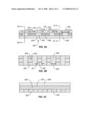
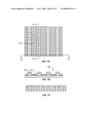
3. The device of claim 2, wherein the at least two solid phases include a generally amorphous phase and a generally crystalline phase.
4. The device of claim 1, wherein the thickness of the insulating member is less than a minimum lithographic feature size for a lithographic process used to form the device.
5. The device of claim 1, wherein the memory material comprises an alloy including a combination of Ge, Sb, and Te.
6. The device of claim 1, wherein the memory material comprises an alloy including a combination of two or more materials from the group of Ge, Sb, Te, Se, In, Ti, Ga, Bi, Sn, Cu, Pd, Pb, Ag, S, and Au.
7. The device of claim 1, wherein the first conductivity type comprises N-type conductivity and the second conductivity type comprises P-type conductivity.
8. The device of claim 1, wherein the first and second electrodes comprise an element selected from a group consisting of Ti, W, Mo, Al, Ta, Cu, Pt, Ir, La, Ni, and Ru and alloys thereof.
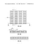
9. The device of claim 1, wherein the first and second electrodes comprise Ti and N.
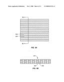
10. The device of claim 1, wherein the first and second electrodes comprise Ta and N.
11. An array of memory cells, the array comprising:a plurality of word lines comprising doped semiconductor material having a first conductivity type, the word lines having word line widths and extending in parallel in a first direction;a plurality of second doped semiconductor regions having a second conductivity type opposite the first conductivity type, second doped semiconductor regions in the plurality of second doped semiconductor regions on corresponding word lines and defining respective pn junctions therebetween;a plurality of electrode pairs, wherein pairs include respective first and second electrodes and an insulating member between the first and second electrodes, the insulating member having a thickness between the first and second electrodes, the first electrodes on corresponding second doped semiconductor regions; andan array of bridges of memory material across the insulating members of respective electrode pairs, the bridges having respective bottom surfaces and contacting the first and second electrodes in the respective electrode pairs on the bottom surface, and defining an inter-electrode path between the corresponding first and second electrodes defined by the thickness of the insulating member, wherein the memory material has at least two solid phases.
12. The array of memory cells of claim 11, wherein the memory cells in the array of memory cells include (a) a pn junction, (b) an electrode pair, and (c) a bridge of memory material, such that the memory cells are arranged in a cross point array.
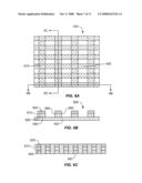
13. The array of memory cells of claim 12, further comprising a plurality of conductive bit lines including second electrodes in the plurality of electrode pairs, the bit lines having bit line widths and extending in parallel in a second direction perpendicular to the first direction.
14. The array of memory cells of claim 13, further comprising:adjacent bit lines in the plurality of bit lines being separated by a first separation distance;adjacent word lines in the plurality of word lines being separated by a second separation distance; andmemory cells in the array of memory cells having a memory cell area, the memory cell area having a first side along the first direction and a second side along the second direction, the first side having a length equal to the word line width and the second separation distance, and the second side having a length equal to the bit line width and the first separation distance.
15. The array of memory cells of claim 14, wherein the first side length is equal to twice a feature size F, and the second side is equal to twice a feature size F, such that the memory cell area is equal to about 4F.sup.2.
16. The array of memory cells of claim 11, wherein the at least two solid phases are reversibly inducible by a current.
17. The array of memory cells of claim 11, wherein the at least two solid phases include a generally amorphous phase and a generally crystalline phase.
18. The array of memory cells of claim 11, wherein the thickness of the insulating member is less than a minimum lithographic feature size for a lithographic process used to form the array.
19. The array of memory cells of claim 11, wherein the memory material comprises an alloy including a combination of Ge, Sb, and Te.
20. The array of memory cells of claim 11, wherein the memory material comprises an alloy including a combination of two or more materials from the group of Ge, Sb, Te, Se, In, Ti, Ga, Bi, Sn, Cu, Pd, Pb, Ag, S, and Au.
21. The array of memory cells of claim 11, wherein the first conductivity type comprises N-type conductivity and the second conductivity type comprises P-type conductivity.
22. The array of memory cells of claim 11, wherein the first and second electrodes comprise an element chosen from a group consisting of Ti, W, Mo, Al, Ta, Cu, Pt, Ir, La, Ni, and Ru and alloys thereof.
23. The array of memory cells of claim 11, wherein the first and second electrodes comprise Ti and N.
24. The array of memory cells of claim 11, wherein the first and second electrodes comprise Ta and N.
25. A method for manufacturing an array of memory cells, the method comprising:forming a plurality of word lines comprising doped semiconductor material having a first conductivity type, the word lines having word line widths and extending in parallel in a first direction;forming a plurality of second doped semiconductor regions, having a second conductivity type opposite the first conductivity type, on corresponding word lines and defining respective pn junctions therebetween;forming a plurality of electrode pairs, wherein pairs include respective first and second electrodes and an insulating member between the first and second electrodes, the insulating member having a thickness between the first and second electrodes, the first electrodes on corresponding second doped semiconductor regions; andforming an array of bridges of memory material across the insulating members of respective electrode pairs, the bridges having respective bottom surfaces and contacting the first and second electrodes in the respective electrode pairs on the bottom surface, and defining an inter-electrode path between the corresponding first and second electrodes defined by the thickness of the insulating member, wherein the memory material has at least two solid phases.
26. The method of claim 25, wherein the memory cells in the array of memory cells include (a) a pn junction, (b) an electrode pair, and (c) a bridge of memory material, such that the memory cells are arranged in a cross point array.
27. The method of claim 26, further comprising forming a plurality of conductive bit lines including second electrodes in the plurality of electrode pairs, the bit lines having bit line widths and extending in parallel in a second direction perpendicular to the first direction.
28. The method of claim 27, further comprising:adjacent bit lines in the plurality of bit lines being separated by a first separation distance;adjacent word lines in the plurality of word lines being separated by a second separation distance; andmemory cells in the array of memory cells having a memory cell area, the memory cell area having a first side along the first direction and a second side along the second direction, the first side having a length equal to the word line width and the second separation distance, and the second side having a length equal to the bit line width and the first separation distance.
29. The method of claim 28, wherein the first side length is equal to twice a feature size F, and the second side length is equal to twice the feature size F, such that the memory cell area is equal to about 4F.sup.2.
30. The method of claim 25, wherein the at least two solid phases are reversibly inducible by a current.
31. The method of claim 25, wherein the at least two solid phases include a generally amorphous phase and a generally crystalline phase.
32. The method of claim 25, wherein the thickness of the insulating member is less than a minimum lithographic feature size for a lithographic process used to form the array.
33. The method of claim 25, wherein the memory material comprises an alloy including a combination of Ge, Sb, and Te.
34. The method of claim 25, wherein the memory material comprises an alloy including a combination of two or more materials from the group of Ge, Sb, Te, Se, In, Ti, Ga, Bi, Sn, Cu, Pd, Pb, Ag, S, and Au.
35. The method of claim 25, wherein the first conductivity comprises N-type conductivity and the second conductivity type comprises P-type conductivity.
36. The method of claim 25, wherein the first and second electrodes comprise an element chosen from a group consisting of Ti, W, Mo, Al, Ta, Cu, Pt, Ir, La, Ni, and Ru and alloys thereof.
37. The method of claim 25, wherein the first and second electrodes comprise Ti and N.
38. The method of claim 25, wherein the first and second electrodes comprise Ta and N.
39. A method for manufacturing an array of memory cells, the method comprising:patterning a multi-layer structure to form a plurality of strips from the multi-layer structure, the strips extending in parallel in a first direction and defining a plurality of first trenches therebetween, wherein the strips in the plurality of strips include (a) a wordline comprising a first doped semiconductor layer having a first conductivity type, (b) a second doped semiconductor layer on the wordline, the second doped semiconductor layer having a second conductivity type, and (c) a conductive bottom electrode layer comprising bottom electrode material on the second doped semiconductor layer;forming a first dielectric material in the plurality of first trenches;forming a plurality of second trenches extending in parallel in a second direction perpendicular to the first direction, thereby exposing portions of the wordlines beneath the second trenches and defining a plurality of multi-layer stacks between the second trenches, the multi-layer stacks having respective top and sidewall surfaces, wherein the multi-layer stacks in the plurality of multi-layer stacks include (a) a second doped region comprising a portion of the second doped semiconductor layer on the corresponding word line and defining a pn junction therebetween, and (b) a first electrode comprising bottom electrode material on the corresponding second doped region;forming a sidewall dielectric layer over the multi-layer stacks and planarizing to expose the top surfaces of the multi-layer stacks, thereby forming a plurality of insulating members on the sidewall surfaces of the multi-layer stacks such that pairs of insulating members are between adjacent first electrodes;forming a plurality of bit lines extending in parallel in the second direction, bit lines in the plurality of bit lines between pairs of insulating members;patterning a layer of memory material to form a plurality of bridges, thereby forming an array of memory cells, the bridges extending across one of the insulating members in the pair of insulating members between adjacent first electrodes, the bridges having respective bottom surfaces and contacting the corresponding first electrodes and bit lines, and defining an inter-electrode path between the corresponding first electrodes and bit lines defined by the thickness of the corresponding insulating member, wherein the memory material has at least two solid phases.
Description:
PARTIES TO A JOINT RESEARCH AGREEMENT
[0001]International Business Machines Corporation, a New York corporation; Macronix International Corporation, a Taiwan corporation, and Infineon Technologies A.G., a German corporation, are parties to a Joint Research Agreement.
BACKGROUND OF THE INVENTION
[0002]1. Field of the Invention
[0003]The present invention relates to high density memory devices based on phase change based memory materials, including chalcogenide based materials and on other programmable resistive materials, and to methods for manufacturing such devices.
[0004]2. Description of Related Art
[0005]Phase change based memory materials are widely used in read-write optical disks. These materials have at least two solid phases, including for example a generally amorphous solid phase and a generally crystalline solid phase. Laser pulses are used in read-write optical disks to switch between phases and to read the optical properties of the material after the phase change.
[0006]Phase change based memory materials, like chalcogenide based materials and similar materials, also can be caused to change phase by application of electrical current at levels suitable for implementation in integrated circuits. The generally amorphous state is characterized by higher resistivity than the generally crystalline state, which can be readily sensed to indicate data. These properties have generated interest in using programmable resistive material to form nonvolatile memory circuits, which can be read and written with random access.
[0007]The change from the amorphous to the crystalline state is generally a lower current operation. The change from crystalline to amorphous, referred to as reset herein, is generally a higher current operation, which includes a short high current density pulse to melt or break down the crystalline structure, after which the phase change material cools quickly, quenching the phase change process, allowing at least a portion of the phase change structure to stabilize in the amorphous state. It is desirable to minimize the magnitude of the reset current used to cause transition of phase change material from the crystalline state to the amorphous state. The magnitude of the reset current needed for reset can be reduced by reducing the size of the phase change material element in the cell and of the contact area between electrodes and the phase change material, so that higher current densities are achieved with small absolute current values through the phase change material element.
[0008]A technology developed by the assignee of the present application is referred to as a phase change bridge cell, in which a very small patch of memory material is formed as a bridge across a thin film insulating member between electrodes. The phase change bridge is easily integrated with logic and other types of circuitry on integrated circuits. See, U.S. application Ser. No. 11/155,067, filed 17 Jun. 2005, entitled "Thin Film Fuse Phase Change RAM and Manufacturing Method," by Lung et al., which application was owned at the time of invention and is currently owned by the same assignee.
[0009]Problems have arisen in manufacturing such devices with very small dimensions, and with variations in process that meet tight specifications needed for large-scale memory devices. It is desirable therefore to provide a memory cell structure with an array architecture supporting high-density devices, and a method for manufacturing such structure that meets tight process variation specifications needed for large-scale memory devices. Furthermore, it is desirable to produce memory devices having a small active phase change region.
SUMMARY OF THE INVENTION
[0010]An array of memory cells described herein includes a plurality of word lines comprising doped semiconductor material having a first conductivity type, the word lines having word line widths and extending in parallel in a first direction. A plurality of second doped semiconductor regions having a second conductivity type opposite the first conductivity type, second doped semiconductor regions in the plurality of second doped semiconductor regions on corresponding word lines and defining respective pn junctions therebetween. A plurality of electrode pairs, wherein pairs include respective first and second electrodes and an insulating member between the first and second electrodes, the insulating member having a thickness between the first and second electrodes, the first electrodes on corresponding second doped semiconductor regions. An array of bridges of memory material across the insulating members of respective electrode pairs, the bridges having respective bottom surfaces and contacting the first and second electrodes in the respective electrode pairs on the bottom surface, and defining an inter-electrode path between the corresponding first and second electrodes defined by the thickness of the insulating member, wherein the memory material has at least two solid phases.
[0011]In preferred embodiments the memory cells have an area equal to 4F2, where F is about one half the sum of the word line width and the separation distance between adjacent word lines, typically about the minimum feature size for a lithographic process used in manufacturing the memory cells.
[0012]A method for manufacturing an array of memory cells as described herein comprises forming a plurality of word lines comprising doped semiconductor material having a first conductivity type, the word lines having word line widths and extending in parallel in a first direction. Forming a plurality of second doped semiconductor regions, having a second conductivity type opposite the first conductivity type, on corresponding word lines and defining respective pn junctions therebetween. Forming a plurality of electrode pairs, wherein pairs include respective first and second electrodes and an insulating member between the first and second electrodes, the insulating member having a thickness between the first and second electrodes, the first electrodes on corresponding second doped semiconductor regions. Forming an array of bridges of memory material across the insulating members of respective electrode pairs, the bridges having respective bottom surfaces and contacting the first and second electrodes in the respective electrode pairs on the bottom surface, and defining an inter-electrode path between the corresponding first and second electrodes defined by the thickness of the insulating member, wherein the memory material has at least two solid phases.
[0013]Other aspects and advantages of the invention are described below with reference to the figures.
BRIEF DESCRIPTION OF THE DRAWINGS
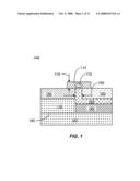
[0014]FIG. 1 illustrates a cross-sectional view of a memory cell having a phase change memory bridge in accordance with an embodiment.
[0015]FIGS. 2A through 2C illustrate cross-sectional views of a portion of an array of memory cells in accordance with an embodiment.
[0016]FIG. 2D illustrates a top view of a portion of the memory array of FIGS. 2A-2C.
[0017]FIGS. 3A through 10C illustrate a fabrication sequence of an array of memory cells in accordance with an embodiment.
DETAILED DESCRIPTION
[0018]The following description of the invention will typically be with reference to specific structural embodiments and methods. It is to understood that there is no intention to limit the invention to the specifically disclosed embodiments and methods but that the invention may be practiced using other features, elements, methods, and embodiments. Preferred embodiments are described to illustrate the present invention, not to limit its scope, which is defined by the claims. Those of ordinary skill in the art will recognize a variety of equivalent variations on the description that follows. Like elements in various embodiments are commonly referred to with like reference numerals.
[0019]A detailed description is provided with reference to FIGS. 1-10.
[0020]FIG. 1 illustrates a cross-sectional view of a memory cell 100 having a phase change memory bridge 110 in accordance with an embodiment. FIG. 1 illustrates a first doped semiconductor region 120 having a first conductivity type and a second doped semiconductor region 130 on the first doped semiconductor region 120, the second doped semiconductor region 130 having a second conductivity type opposite the first conductivity type. The interface between the first doped semiconductor region 120 and the second doped semiconductor region 130 defines a pn junction 140. In the illustrated embodiment the first semiconductor region 120 comprises N-type conductivity and the second semiconductor region 130 comprises P-type conductivity. In some alternative embodiments, the first semiconductor region 120 comprises P-type conductivity and the second semiconductor region 130 comprises N-type conductivity. The first and second semiconductor regions 120, 130 in some embodiments comprises a conductivity having a gradient doping. For example, a semiconductor region having N-type conductivity may include N.sup.+ and N.sup.- doped regions and a semiconductor region having P-type conductivity may include P.sup.+ and P.sup.- doped regions.
[0021]A first electrode 150 comprising conductive material is on the second doped semiconductor region 140. An insulating member 155 has a thickness 165 between the first electrode 150 and a conductive second electrode 160. The bridge of memory material 110 is across the insulating member 155 and contacts the first and second electrodes 150,160 on a bottom surface of the bridge 110. In operation, voltages on the first doped semiconductor region 120 and the second electrode 160 can induce current to flow from the first doped semiconductor region 120 to the second electrode 160, or vice-versa, via the second doped semiconductor region 130, the first electrode 150, and the bridge 110 of memory material.
[0022]The active region 170 is the region of the bridge 110 in which the memory material is induced to change between at least two solid phases. As can be appreciated the active region 170 can be made extremely small in the illustrated structure, reducing the magnitude of current needed to induce the phase changes. The inter-electrode path length between the first and second electrodes 150, 160 is defined by the thickness 165 of the insulating member. In representative embodiments, the thickness 165 of the insulating member 155 can be established using a thin film deposition technique to form a thin sidewall dielectric on the sidewall of first electrode 150. Likewise, the thickness 115 of the bridge 110 of memory material can be very small. The thickness 115 can be established using a thin film deposition technique of memory material on the top surfaces of the first electrode 150, the insulating member 110, and the second electrode 160.
[0023]In the illustrated embodiment a dielectric layer 180 is between the first doped semiconductor region 120 and the insulating member 155. Alternatively, the dielectric layer 180 can be omitted such that the insulating member 155 is on the first doped semiconductor region 120.
[0024]Embodiments of the memory cell 100 include phase change based memory materials, including chalcogenide based materials and other materials, for the bridge 110. Chalcogens include any of the four elements oxygen (O), sulfur (S), selenium (Se), and tellurium (Te), forming part of group VI of the periodic table. Chalcogenides comprise compounds of a chalcogen with a more electropositive element or radical. Chalcogenide alloys comprise combinations of chalcogenides with other materials such as transition metals. A chalcogenide alloy usually contains one or more elements from column six of the periodic table of elements, such as germanium (Ge) and tin (Sn). Often, chalcogenide alloys include combinations including one or more of antimony (Sb), gallium (Ga), indium (In), and silver (Ag). Many phase change based memory materials have been described in technical literature, including alloys of: Ga/Sb, In/Sb, In/Se, Sb/Te, Ge/Te, Ge/Sb/Te, In/Sb/Te, Ga/Se/Te, Sn/Sb/Te, In/Sb/Ge, Ag/In/Sb/Te, Ge/Sn/Sb/Te, Ge/Sb/Se/Te and Te/Ge/Sb/S. In the family of Ge/Sb/Te alloys, a wide range of alloy compositions may be workable. The compositions can be characterized as TeaGebSb.sub.100-(a+b).
[0025]One researcher has described the most useful alloys as having an average concentration of Te in the deposited materials well below 70%, typically below about 60% and ranged in general from as low as about 23% up to about 58% Te and most preferably about 48% to 58% Te. Concentrations of Ge were above about 5% and ranged from a low of about 8% to about 30% average in the material, remaining generally below 50%. Most preferably, concentrations of Ge ranged from about 8% to about 40%. The remainder of the principal constituent elements in this composition was Sb. These percentages are atomic percentages that total 100% of the atoms of the constituent elements. (Ovshinsky '112 patent, cols 10-11.) Particular alloys evaluated by another researcher include Ge2Sb2Te5, GeSb2Te4 and GeSb4Te7, (Noboru Yamada, "Potential of Ge--Sb--Te Phase-Change Optical Disks for High-Data-Rate Recording", SPIE v.3109, pp. 28-37 (1997).) More generally, a transition metal such as chromium (Cr), iron (Fe), nickel (Ni), niobium (Nb), palladium (Pd), platinum (Pt) and mixtures or alloys thereof may be combined with Ge/Sb/Te to form a phase change alloy that has programmable resistive properties. Specific examples of memory materials that may be useful are given in Ovshinsky '112 at columns 11-13, which examples are hereby incorporated by reference.
[0026]Phase change alloys are capable of being switched between a first structural state in which the material is in a generally amorphous solid phase, and a second structural state in which the material is in a generally crystalline solid phase in its local order in the active channel region of the cell. These alloys are at least bistable. The term amorphous is used to refer to a relatively less ordered structure, more disordered than a single crystal, which has the detectable characteristics such as higher electrical resistivity than the crystalline phase. The term crystalline is used to refer to a relatively more ordered structure, more ordered than in an amorphous structure, which has detectable characteristics such as lower electrical resistivity than the amorphous phase. Typically, phase change materials may be electrically switched between different detectable states of local order across the spectrum between completely amorphous and completely crystalline states. Other material characteristics affected by the change between amorphous and crystalline phases include atomic order, free electron density and activation energy. The material may be switched either into different solid phases or into mixtures of two or more solid phases, providing a gray scale between completely amorphous and completely crystalline states. The electrical properties in the material may vary accordingly.
[0027]Phase change alloys can be changed from one phase state to another by application of electrical pulses. It has been observed that a shorter, higher amplitude pulse tends to change the phase change material to a generally amorphous state. A longer, lower amplitude pulse tends to change the phase change material to a generally crystalline state. The energy in a shorter, higher amplitude pulse is high enough to allow for bonds of the crystalline structure to be broken and short enough to prevent the atoms from realigning into a crystalline state. Appropriate profiles for pulses can be determined empirically or by modeling, and specifically adapted to a particular phase change alloy. In following sections of the disclosure, the phase change material is referred to as GST, and it will be understood that other types of phase change materials can be used. A material useful for implementation of a PCRAM described herein is Ge2Sb2Te5.
[0028]The following are short summaries describing four types of resistive memory materials.
1. Chalcogenide material [0029]GexSbyTez [0030]x:y:z=2:2:5 [0031]Or other compositions with x: 0˜5; y: 0˜5; z: 0˜10 [0032]GeSbTe with doping, such as N--, Si--, Ti--, or other element doping may also be used. [0033]Formation method: By PVD sputtering or magnetron-sputtering method with reactive gases of Ar, N2, and/or He, etc chalcogenide @ the pressure of 1 mtorr˜100 mtorr. The deposition is usually done at room temperature. The collimator with aspect ratio of 1˜5 can be used to improve the fill-in performance. To improve the fill-in performance, the DC bias of several ten to several hundred volts is also used. On the other hand, the combination of DC bias and the collimator can be used simultaneously. [0034]The post deposition annealing treatment with vacuum or N2 ambient is sometimes needed to improve the crystallize state of chalcogenide material. The annealing temperature typically ranges 100 C. to 400 C with an anneal time of less than 30 minutes. [0035]The thickness of chalcogenide material depends on the design of cell structure. In general, a chalcogenide material with thickness of higher than 8 nm can have a phase change characterization so that the material exhibits at least two stable resistance states.2. CMR (colossal magneto resistance) material [0036]PrxCayMnO3 [0037]x:y=0.5:0.5 [0038]Or other compositions with x: 0˜1; y: 0˜1 [0039]Another CMR material that includes Mn oxide may be used [0040]Formation method: By PVD sputtering or magnetron-sputtering method with reactive gases of Ar, N2, O2, and/or He, etc. at the pressure of 1 mtorr˜100 mtorr. The deposition temperature can range from room temperature to ˜600 C, depending on the post deposition treatment condition. A collimator with an aspect ratio of 1˜5 can be used to improve the fill-in performance. To improve the fill-in performance, the DC bias of several ten to several hundred volts is also used. On the other hand, the combination of DC bias and the collimator can be used simultaneously. A magnetic field of several ten gauss to 10,000 gauss may be applied to improve the magnetic crystallized phase. [0041]The post deposition annealing treatment with vacuum or N2 ambient or O2/N2 mixed ambient may be needed to improve the crystallized state of CMR material. The annealing temperature typically ranges 400 C to 600 C with an anneal time of less than 2 hours. [0042]The thickness of CMR material depends on the design of cell structure. The CMR thickness of 10 nm to 200 nm can be used to be the core material. [0043]A buffer layer of YBCO (YBaCuO3, a kind of high temperature superconductor material) is often used to improve the crystallized state of CMR material. The YBCO is deposited before the deposition of CMR material. The thickness of YBCO ranges 30 nm to 200 nm.3.2-element compound [0044]NixOy; TixOy; AlxOy; WxOy; ZnxOy; ZrxOy; CuxOy; etc [0045]x:y=0.5:0.5 [0046]Other compositions with x: 0˜1; y: 0˜1 [0047]Formation method: [0048]1. Deposition: By PVD sputtering or magnetron-sputtering method with reactive gases of Ar, N2, O2, and/or He, etc. at the pressure of 1 mtorr˜100 mtorr, using a target of metal oxide, such as NixOy; TixOy; AlxOy; WxOy; ZnxOy; ZrxOy; CuxOy; etc. The deposition is usually done at room temperature. A collimator with an aspect ratio of 1˜5 can be used to improve the fill-in performance. To improve the fill-in performance, the DC bias of several ten to several hundred volts is also used. If desired, they combination of DC bias and the collimator can be used simultaneously. [0049]The post deposition annealing treatment with vacuum or N2 ambient or O2/N2 mixed ambient as sometimes needed to improve the oxygen distribution of metal oxide. The annealing temperature ranges 400 C to 600 C with an anneal time of less than 2 hours. [0050]2. Reactive deposition: By PVD sputtering or magnetron-sputtering method with reactive gases of Ar/O2, Ar/N2/O2, pure O2, He/O2, He/N2/O2 etc. at the pressure of 1 mtorr˜100 mtorr, using a target of metal oxide, such as Ni, Ti, Al, W, Zn, Zr, or Cu etc. The deposition is usually done at room temperature. A collimator with an aspect ratio of 1˜5 can be used to improve the fill-in performance. To improve the fill-in performance, a DC bias of several ten to several hundred volts is also used. If desired, the combination of DC bias and the collimator can be used simultaneously. [0051]The post deposition annealing treatment with vacuum or N2 ambient or O2/N2 mixed ambient is sometimes needed to improve the oxygen distribution of metal oxide. The annealing temperature ranges 400 C to 600 C with an anneal time of less than 2 hours. [0052]3. Oxidation: By a high temperature oxidation system, such as furnace or RTP system. The temperature ranges from 200 C to 700 C with pure O2 or N2O2 mixed gas at a pressure of several mtorr to 1 atm. The time can range several minute to hours. Another oxidation method is plasma oxidation. An RF or a DC source plasma with pure O2 or Ar/O2 mixed gas or Ar/N2/O2 mixed gas at a pressure of 1 mtorr to 100 mtorr is used to oxidize the surface of metal, such as Ni, Ti, Al, W, Zn, Zr, or Cu etc. The oxidation time ranges several seconds to several minutes. The oxidation temperature ranges room temperature to 300 C, depending on the degree of plasma oxidation.4. Polymer material [0053]TCNQ with doping of Cu, C60, Ag etc. [0054]PCBM-TCNQ mixed polymer [0055]Formation method: [0056]1. Evaporation: By thermal evaporation, e-beam evaporation, or molecular beam epitaxy (MBE) system. A solid-state TCNQ and dopant pellets are co-evaporated in a single chamber. The solid-state TCNQ and dopant pellets are put in a W-boat or a Ta-boat or a ceramic boat. A high electrical current or an electron-beam is applied to melt the source so that the materials are mixed and deposited on wafers. There are no reactive chemistries or gases. The deposition is done at a pressure of 10-4 torr to 10-10 torr. The wafer temperature ranges from room temperature to 200 C. [0057]The post deposition annealing treatment with vacuum or N2 ambient is sometimes needed to improve the composition distribution of polymer material. The annealing temperature ranges room temperature to 300 C with an anneal time of less than 1 hour. [0058]2. Spin-coat: By a spin-coater with the doped-TCNQ solution @ the rotation of less than 1000 rpm. After spin-coating, the wafer is put to wait the solid-state formation @ room temperature or temperature of less than 200 C. The waiting time ranges from several minutes to days, depending on the temperature and on the formation conditions.
[0059]An exemplary method for forming chalcogenide material uses the PVD-sputtering or magnetron-sputtering method with source gas(es) of Ar, N2, and/or He, etc. at the pressure of 1 mTorr ˜100 mTorr. The deposition is usually done at room temperature. A collimator with an aspect ratio of 1˜5 can be used to improve the fill-in performance. To improve the fill-in performance, a DC bias of several tens of volts to several hundreds of volts is also used. On the other hand, the combination of DC bias and the collimator can be used simultaneously.
[0060]A post-deposition annealing treatment in vacuum or in an N2 ambient is optionally performed to improve the crystallize state of chalcogenide material. The annealing temperature typically ranges from 100° C. to 400° C. with an anneal time of less than 30 minutes.
[0061]The thickness of chalcogenide material depends on the design of cell structure. In general, a chalcogenide material with thickness of higher than 8 nm can have a phase change characterization so that the material exhibits at least two stable resistance states. It is expected that some materials are suitable with even lower thicknesses.
[0062]FIGS. 2A-2C are cross-sectional views of a portion of a cross-point array of memory cells in accordance with an embodiment. FIG. 2A is a cross-section taken orthogonal to bit lines 260 and include a plurality of memory cells 200. FIG. 2B and FIG. 2C are cross-sections taken orthogonal to word lines 220.
[0063]Word lines 220 extend in parallel in a first direction, the word lines 220 having word line widths 201 and adjacent word lines 220 separated by a word line separation distance 202. The word lines 220 comprise doped semiconductor material having a first conductivity type. Conductive bit lines 260 extend in parallel in a second direction perpendicular to the first direction, the bit lines 260 having bit line widths 261 and adjacent bit lines being separated by a bit line separation distance 262. In the illustrated embodiment the bit lines 260 form the second electrodes of the memory cells 200. Dielectric material 290 is between adjacent word lines 220.
[0064]The memory cells 200 include second doped semiconductor regions 230 on the corresponding word line 220 and define respective pn junctions 240 therebetween. The second doped semiconductor regions 230 have a second doped conductivity type opposite the first conductivity type. The memory cells 200 include electrode pairs, the pairs including respective first electrodes 250 and second electrodes (bit lines 260) and an insulating member 255 between the first electrode 250 and the second electrodes (bit lines 260), the first electrodes 250 on the corresponding second doped semiconductor regions 230. The insulating member 255 has a thickness 256 between the first electrodes 250 and the second electrodes (bit lines 260). In the illustrated embodiment dielectric 280 is between the insulating members 255 and the word lines 220. Alternatively, the dielectric 280 can be omitted such that the insulating members 255 are on the corresponding word lines 220.
[0065]The memory cells 200 include a bridge 210 of memory material across the insulating member 255. The bridge 210 has a bottom surface and contacts the first electrodes 250 and the second electrodes (bit lines 260) on the bottom surface. An inter-electrode path between the first electrodes 250 and the second electrodes (bit lines 260) has a path length defined by the thickness 256 of the insulating member 255.
[0066]The bridges 210 in the illustrated embodiment comprise memory material having at least two solid phases that are reversible, such as chalcogenide material or other related material, by applying a current through the bridge 210 or applying a voltage across the first electrodes 250 and the second electrodes (bit lines 260).
[0067]It will be understood that a wide variety of materials can be utilized in implementation of the conductive bit lines 260 and first electrodes 250, including metals such as aluminum, titanium nitride, and tungsten based materials as well as non-metal conductive material such as doped polysilicon. The first electrodes 250 and bit lines 260 in the illustrated embodiment are preferably TiN or TaN. Alternatively, the first electrodes 250 and bit lines 260 are TiAlN or TaAlN, or comprise, for further examples, one or more elements selected from the group consisting of Ti, W, Mo, Al, Ta, Cu, Pt, Ir, La, Ni, and Ru and alloys thereof.
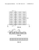
[0068]FIG. 2D is a top view, or plan view, of the array of memory cells 200 illustrated in FIGS. 2A-2C. Memory cells 200 have a memory cell area 295. In preferred embodiments the summation of the bit line width 261 and the bit line separation distance 262 is equal to about twice a feature size F, and F preferably being a minimum feature size for the lithographic process used to create the word lines 220 and bit lines 260; and the summation of the word line width 201 and the word line separation distance 202 is equal to about twice the feature size F, such that the memory cells have an area 295 equal to 4F2.
[0069]FIGS. 3-10 illustrate an embodiment of a process flow for manufacturing a memory array, utilizing a memory cell as described herein. FIGS. 3A-3B illustrate respective top and cross-sectional views of a multi-layer structure 300 including a first doped semiconductor layer 310, a second doped semiconductor layer 320, and a conductive bottom electrode layer 330. The first and second doped semiconductor layers 310, 320 have respective first and second conductivity types, the first conductivity type opposite the second conductivity type.
[0070]Next, the multi-layer structure 300 illustrated in FIGS. 3A-3B is patterned, resulting in the structure illustrated in FIGS. 4A-4B having a plurality of strips 400 extending in parallel in a first direction and defining first trenches 410 between the strips 400. The strips 400 include word lines 420 comprising a portion of the first doped semiconductor layer 310.
[0071]Next, a first dielectric material 500 is formed in the first trenches 410 of the structure illustrated in FIGS. 4A-4B and planarized, using for example chemical mechanical polishing CMP, resulting in the structure illustrated in FIGS. 5A-5B. The first dielectric material 500 can comprise, for example, silicon dioxide.
[0072]Next, a plurality of second trenches 600 are formed by etching the structure illustrated in FIGS. 5A-5B, resulting in the structure illustrated in FIGS. 6A-6C having a plurality of multi-layer stacks 610 between the second trenches 600. The second trenches 600 extend in parallel in a second direction perpendicular to the first direction. As can be seen in FIGS. 6A-6C, the portions of the wordlines 420 beneath the trenches 600 are exposed. The multi-layer stacks 610 include a second doped region 620 and a first electrode 630. The second doped region 620 comprises a portion of the second doped semiconductor region 320 on the corresponding word line 420 and defines a pn junction 640 therebetween. The first electrode 630 comprises the bottom electrode layer 330 on the corresponding second doped region 620. The multi-layer stacks 610 have sidewall surfaces 660.
[0073]Next, a second dielectric material 700 is formed in the trenches 600 of FIGS. 6A-6C, the second dielectric material 700 partially filling the trenches 600 and resulting in the structure illustrated in FIGS. 7A-7C. The second dielectric material 700 can be formed for example, by filling the trenches 600 with dielectric material 700 and selectively etching back the dielectric material 700.
[0074]Next, a conformal layer of a third dielectric material is formed on the structure illustrated in FIGS. 7A-7C and planarized, using for example CMP, to expose the top surface 810 of the multi-layer stack 610, resulting in the structure illustrated in FIGS. 8A-8C having insulating members 820 on the sidewalls 660 of the stacks 610. As can been seen in FIG. 8B, pairs of insulating members 820 are between adjacent first electrodes 630.
[0075]Next, a layer of conductive material is formed on the structure illustrated in FIGS. 8A-8C and planarized, using for example CMP, resulting in the structure illustrated in FIGS. 9A-9C having bit lines 900 extending in parallel in the second direction, the bit lines 900 between pairs of insulating members 820. Next, a layer of phase change material is patterned to form a plurality of phase change bridges 1000 as illustrated in FIGS. 10A-10C, resulting in the array of memory cells as illustrated in FIGS. 2A-2D. Alternatively, the phase change bridges 1000 may be formed, for example, by patterning a layer of dielectric material over the structure illustrated in FIGS. 9A-9C and using that layer of dielectric material as a mask for forming the phase change bridges 1000.
[0076]An embodiment of an array of memory cells as described herein include a plurality of word lines comprising doped semiconductor material having a first conductivity type, the word lines having word line widths and extending in parallel in a first direction. A plurality of second doped semiconductor regions having a second conductivity type opposite the first conductivity type, second doped semiconductor regions in the plurality of second doped semiconductor regions on corresponding word lines and defining respective pn junctions therebetween. A plurality of electrode pairs, wherein pairs include respective first and second electrodes and an insulating member between the first and second electrodes, the insulating member having a thickness between the first and second electrodes, the first electrodes on corresponding second doped semiconductor regions. An array of bridges of memory material across the insulating members of respective electrode pairs, the bridges having respective bottom surfaces and contacting the first and second electrodes in the respective electrode pairs on the bottom surface, and defining an inter-electrode path between the corresponding first and second electrodes defined by the thickness of the insulating member, wherein the memory material has at least two solid phases.
[0077]Advantages of an embodiment described herein include memory cells having reduced cell sizes, providing an array architecture supporting high-density devices, and a method for manufacturing such structure that meets tight process variation specifications needed for large-scale memory devices.
[0078]While the present invention is disclosed by reference to the preferred embodiments and examples detailed above, it is to be understood that these examples are intended in an illustrative rather than in a limiting sense. It is contemplated that modifications and combinations will occur to those skilled in the art, which modifications and combinations will be within the spirit of the invention and the scope of the following claims.
[0079]Any and all patents, patent applications and printed publications referred to above are incorporated by reference. What is claimed is:
User Contributions:
comments("1"); ?> comment_form("1"); ?>Inventors list |
Agents list |
Assignees list |
List by place |
Classification tree browser |
Top 100 Inventors |
Top 100 Agents |
Top 100 Assignees |
Usenet FAQ Index |
Documents |
Other FAQs |
User Contributions:
Comment about this patent or add new information about this topic:
Images included with this patent application:
 |  |
 |  |
 |  |
 |  |
 |  |
 |  |
| Similar patent applications: | |
| Date | Title |
|---|---|
| 2011-08-11 | Phase change device with offset contact |
| 2010-01-14 | Battery-less cache memory module with integrated backup |
| 2011-10-20 | Memory cells with rectifying device |
| 2012-12-27 | Low voltage metal gate antifuse with depletion mode mosfet |
| 2013-06-06 | Battery-less cache memory module with integrated backup |
| New patent applications in this class: | |
| Date | Title |
|---|---|
| 2019-05-16 | Resistive memory device |
| 2017-08-17 | Memory cell architecture for multilevel cell programming |
| 2017-08-17 | Dual demarcation voltage sensing before writes |
| 2016-12-29 | Hardware apparatuses and methods to check data storage devices for transient faults |
| 2016-09-01 | Set and reset operation in phase change memory and associated techniques and configurations |
| New patent applications from these inventors: | |
| Date | Title |
|---|---|
| 2014-06-05 | Uniform critical dimension size pore for pcram application |
| 2014-03-06 | Integrated circuit including vertical diode |
| 2011-10-06 | Stacked bit line dual word line nonvolatile memory |
| 2010-12-23 | Memory device and method for sensing and fixing margin cells |
| 2010-11-25 | Phase change memory cell having vertical channel access transistor |
| Top Inventors for class "Static information storage and retrieval" | |
| Rank | Inventor's name |
|---|---|
| 1 | Frankie F. Roohparvar |
| 2 | Vishal Sarin |
| 3 | Roy E. Scheuerlein |
| 4 | Yan Li |
| 5 | Yiran Chen |